Is the Silicon EPI Wafer Market Powering the Next Semiconductor Leap?
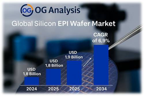
As the digital age pushes the boundaries of speed, efficiency, and miniaturization, silicon epitaxial (EPI) wafers have become the bedrock of high-performance semiconductor devices. These engineered wafers, essential for power semiconductors, MEMS, and LEDs, enable superior control over device architecture and electrical properties. According to OG Analysis, the Global Silicon EPI Wafer Market is valued at USD 1.8 billion in 2024, projected to reach USD 1.9 billion in 2025, and is expected to grow at a CAGR of 6.9%, reaching USD 3.4 billion by 2034.
1. Why Are Silicon EPI Wafers Crucial for Next-Gen Electronics?
Epitaxial wafers offer a controlled crystal layer that enhances carrier mobility, power handling, and device reliability. They are indispensable in power electronics, RF devices, and MEMS sensors, where device precision and performance are paramount. As global demand rises for electric vehicles, 5G infrastructure, and smart medical devices, the EPI wafer market is stepping into the spotlight.
2. What Are the Latest Technological Breakthroughs in EPI Processes?
Processes like Chemical Vapor Deposition (CVD) and Molecular Beam Epitaxy (MBE) are being refined to enable defect-free layers and advanced doping techniques. Leading manufacturers such as SUMCO, GlobalWafers, and Siltronic AG are investing in ultra-thin layer deposition and wafer uniformity enhancement—vital for producing high-voltage and high-frequency semiconductor chips.
3. Which Wafer Sizes Are Driving Market Demand—and Why?
- 12-inch wafers are emerging as the industry standard for high-volume production, especially in advanced power and logic chips.
- 8-inch wafers maintain strong adoption in MEMS, RF, and analog circuits, driven by stable demand from automotive and industrial sectors.
- Smaller wafers like 6-inch still hold relevance in legacy applications and prototyping.
With the rise of silicon carbide and gallium nitride semiconductors, customized wafer formats may also gain prominence in specific verticals.
Click Here for the Full Market Report:
4. Which Applications Are Catalysing the EPI Wafer Surge?
- LEDs continue to drive steady demand, especially in automotive lighting and display panels.
- Power semiconductors are booming, fuelled by EV drivetrain electrification, renewable energy infrastructure, and smart grids.
- MEMS-based devices, such as sensors and actuators, are exploding in wearables, industrial robotics, and medical tech.
These diverse applications are helping silicon EPI wafers become a strategic enabler of tech evolution across sectors.
5. How Are Key Players Positioning for Competitive Advantage?
Top-tier players such as Shin-Etsu Chemical, TSMC, Episil Technologies, and Okmetic are enhancing their foothold through:
- Vertical integration of wafer production and epitaxy
- Strategic partnerships with fabless chipmakers and foundries
- Capacity expansion in high-growth regions like Southeast Asia and Eastern Europe
- Customized wafer offerings to address niche applications in automotive and telecom sectors
Innovation in process scalability and yield improvement is becoming a key differentiator.
6. Which Regions Are Leading—and Which Ones Are Catching Up?
- Asia-Pacific dominates the market, led by Taiwan, China, South Korea, and Japan, which house major fabs and foundries.
- North America is a major consumer, especially in automotive tech and aerospace electronics.
- Europe is investing in semiconductor sovereignty, with strong support for local chip manufacturing ecosystems.
- Middle East and Latin America are early-stage markets, but strategic for future fab expansions and diversification.
The global chip race is turning regional self-reliance and secure supply chains into a strategic priority.
Click Here for the Full Market Report:
7. What Are the Emerging Opportunities for Growth and Innovation?
- Automotive electrification is a multi-billion-dollar opportunity for high-voltage, low-loss EPI wafers.
- Healthcare electronics, including implantables and remote diagnostics, are demanding ultra-reliable sensors built on EPI substrates.
- Telecommunications, particularly with 6G on the horizon, will require high-frequency RF chipsets built on engineered wafers.
- Sustainable manufacturing and recycled wafer solutions are also opening ESG-aligned innovation pathways.
Key Segments of the Silicon EPI Wafer Market Driving Opportunities and Innovations?
By Application:
LED
Power Semiconductor
MEMS-based Devices
By Process:
CVD
Liquid Phase Epitaxy
Molecular Beam Epitaxy
By Wafer Size:
6-inch
8-inch
12-inch
Others
By End-Use Industry:
Consumer Electronics
Telecommunications
Automotive
Healthcare
Industrial
Others
By Geography:
North America (USA, Canada, Mexico)
Europe (Germany, UK, France, Spain, Italy, Rest of Europe)
Asia-Pacific (China, India, Japan, Australia, Rest of APAC)
The Middle East and Africa (Middle East, Africa)
South and Central America (Brazil, Argentina, Rest of SCA)
Browse through More Reports Similar to the Silicon EPI Wafer Market 2025, By the OG Analysis:
Silicon Market Analysis and Outlook Report:
Global Liquid Crystal on Silicon Market Outlook Report:
Connect with us on:
Phone: +91 888 64 99099
Email: mailto:[email protected]
Learn More about OG Analysis
OG Analysis, established in 2009 has 14+ years of experience and served 1800+ clients from 980+ companies operating in 54+ countries. OG Analysis is a leading provider of market research reports in Chemicals, Energy, Oil & Gas, Food & Beverage, Electronics & Semiconductors, Automotive, Telecommunication, Healthcare and Other industries.